G2-1: Transistor Characteristics
Apparatus
\(3\text{V}\) battery; \(9\text{V}\) battery; 2 rheostats (high resistance); resistor \(\text{R}_2\) (approx. \(50\text{k}\Omega\)); voltmeter (\(0-5\text{Vdc}\)); ammeter (\(\approx 50 \mu\text{A}\) fsd); ammeter (\(\approx 3 \text{mA}\) fsd); transistor (pnp); connecting leads (12 short); 2 sheets graph paper.
Instructions
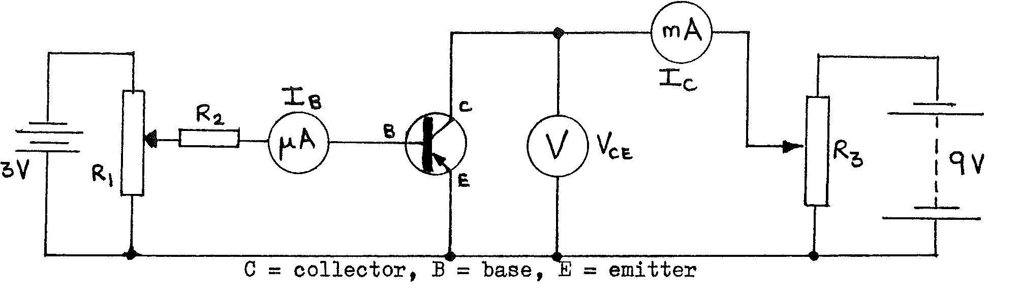
Set up the circuit as above, but do not connect the batteries until a teacher has checked the circuit (to avoid damaging the ammeters or transistor). In the experiment, when not taking readings, leave the batteries disconnected.
Experiment 1
To investigate the ‘transfer characteristics’ of the transistor. The transistor acts as a current amplifier: the size of the large current \(I_C\) depends on the size of the small current \(I_B\). The circuit used above is called a ‘common emitter’ circuit.
1: Procedure
- Set \(V_{CE}\) to \(4\text{V}\) using rheostat \(\text{R}_3\). Ensure that this remains constant (adjust \(\text{R}_3\) again later as necessary).
- Set \(I_B\) to 0 using \(\text{R}_1\). Read and note \(I_B\) and \(I_C\).
- Increase \(I_B\) a little using \(\text{R}_1\), and read and note \(I_B\) and \(I_C\). Continue increasing \(I_B\) and reading the ammeters until \(I_C =\) 3 mA.
- Tabulate the readings of \(I_E\), \(I_C\), and the value of \(V_{CE}\).
1: Analysis
Plot a graph of \(I_C\) against \(I_B\), labelling the curve with the value of \(V_{CE}\) used.
Find the gradient of the straight-line section of the curve. Then:
\[\text{Current gain } \beta = \frac{\Delta I_C}{\Delta I_B} = \text{gradient}\]
Experiment 2
To study how \(I_C\) varies when \(V_{CE}\) is changed, for certain fixed values of \(I_B\). The graph obtained is called the ’output characteristic’ of the transistor.
2: Procedure
- Set \(I_B = 0\) using \(\text{R}_1\). Starting with \(V_{CE} = 0\), and little by little increasing \(V_{CE}\) up to \(5\text{V}\), take a set of readings of \(I_C\) and \(V_{CE}\) and note the value of \(I_B = 0\).
- Increase \(I_B\) to \(10 \mu\)A, and obtain another set of readings of \(I_C\) and \(V_{CE}\) as in step 1.
- Repeat the procedure with \(I_B = 20 \mu\)A then \(30 \mu\)A.
- Tabulate the sets of readings of \(I_C\) and \(V_{CE}\), noting the value of \(I_B\) for each set.
2: Analysis
- Plot a graph of \(I_C\) vs. \(V_{CE}\) to obtain four curves. Label each curve with the appropriate value of \(I_B\) used.
Questions
When \(I_B = 0\), \(I_C\) should be zero for all \(V_{CE}\). However all transistors have some leakage current. What is the value of the leakage current \(I_C\) when \(V_{CE} = 4\)V?
What is the approximate minimum \(V_{CE}\) so that a variation in \(I_B\) between \(0\) and \(30 \mu A\) produces a large change in \(I_C\)? (In practice the supply voltage is usually set between this value and a certain maximum. The maximum depends on the ‘breakdown voltage’ of the junctions).
In use as an amplifier, an AC input voltage makes \(I_B\) vary with time. For example:
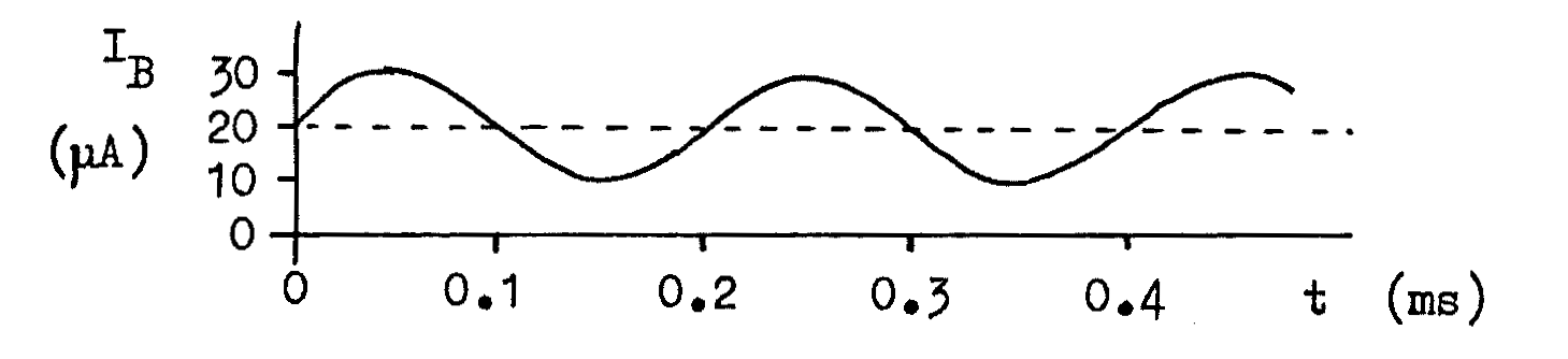
- Use the value of \(\beta\) to make a graph of \(I_C\) against time.
- If a resistor \(\text{R} = 1\)k\(\Omega\) is connected in
- series with the collector \(C\), so that \(I_C\) flows through it; draw a graph of the potential difference (p.d.) across this resistor against time.
- What is the frequency of these AC currents and p.d.?
Draw a diagram to show while the pnp transistor is conducting:
- Electron flows and conventional currents through the three terminals.
- Electron & hole movements inside the transistor (may be simplified).